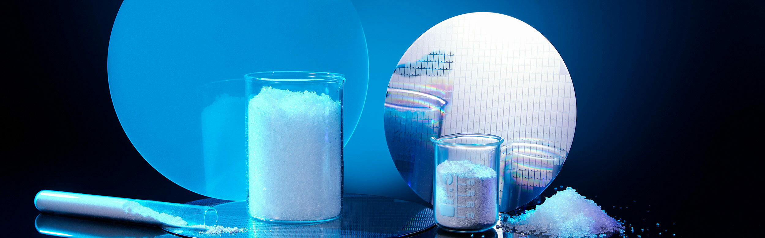
Recent analysis from UBS into the future of AI infrastructure and semiconductor demand has reinforced the growing importance of high-purity materials — including High Purity Alumina (HPA) — in enabling next-generation technologies.
Alpha HPA is referenced in the report (page 8) in the context of advanced semiconductor applications, particularly where performance, reliability and material purity are critical.
Key insights highlighted include:
- Thermal management for AI chips
As AI and data centre workloads increase, managing heat is a critical challenge. HPA-based materials offer thermal conductivity up to 30 times higher than traditional silica, supporting more efficient cooling of high-performance chips. - Ultra-low alpha radiation purity
Alpha HPA’s proprietary process achieves uranium and thorium levels below one part per billion. This “low-alpha” purity is essential in preventing data errors and premature failure in advanced semiconductor devices. - Advanced wafer polishing (CMP)
HPA is used in chemical mechanical planarisation processes for materials such as silicon carbide (SiC) and gallium nitride (GaN), with Alpha HPA materials demonstrating significantly higher removal rates — enabling faster and more efficient manufacturing. - Durability in semiconductor equipment
HPA is also used in critical equipment components exposed to extreme conditions. Its hardness, thermal stability and resistance to corrosive environments contribute to longer equipment life and improved production yields.
As demand for AI-enabled technologies continues to accelerate, materials like HPA are becoming increasingly important in supporting the performance and reliability of global semiconductor supply chains.
Read the full report with a UBS registered email here.


